For my first post on SystemVerilog real number modeling (SVRNM), I decided to discuss a simple circuit—specifically, the sample and hold. To make it more interesting, I introduced two non-ideal parameters to the model: limited bandwidth and a maximum output voltage. Plus, I threw in some noise during both the sample and hold phases for an added layer of complexity.
This component will be a part of a more intricate model, specifically the pipeline ADC. The sample and hold function is the initial stage in this ADC.
Following is the schematic of the cell

During the sample phase, the Q1 and Q2 switches are turned on, while Q3 is off. The capacitors get charged from the input source during this time. When it's the hold phase, the switches change states, and the output voltage becomes equal to the sampled input voltage.
Following is the pin list of the cell, for some of the pins I used the Cadence cds_rnm_pkg and EE_pkg packages. this packages include special user net types (UDN) with several resolution function (UDR) suitable for real number modeling, you can find all about these nettypes in this free online course "SystemVerilog Real Number Modeling (SV-RNM) Advanced Verification".
Pin name | Direction | Pin type | Function |
|---|---|---|---|
vdd | inout | EEnet | positive supply |
vss | inout | EEnet | ground |
en | input | logic | enable |
inp | input | wreal4State | positive input |
inm | input | wreal4State | negative input |
samp | input | logic | sample |
hold | input | logic | hold |
outp | outp | wreal4State | positive output |
outm | outp | wreal4State | negative output |
vcm | input | wreal4State | common mode voltage |
Here is the primary code responsible for creating this model. The complete code and test bench are available in this GitHub repository.
Noise contribution:
While the cell is in sample mode, the input capacitors gather noise from the operational amplifier. The total accumulated noise depends on the opamp noise factor and the capacitor size. In the code, I simply used 1uV as the standard deviation for the noise.
The hold stage in the code follows a similar approach. I distinguish the noise contribution between phases because in a switch capacitor circuit, the noise impact varies between phases. This separation enables the model to more precisely represent the noise contribution.
parameter real InNsStd = 1.0e-6; // Input Noise standard deviation parameter real outNsStd = 1.0e-6; // Output Noise standard deviation
int seedp = 123; int seedm = 456;
always @ (posedge samp) begin sampInt = ((inp + InNsStd * $dist_normal(seedp,0,33))
-
(inm + InNsStd * $dist_normal(seedm,0,33)));
end
always @ (posedge hold) begin outReal = sampInt + outNsStd * $dist_normal(seedm,0,33); end
Finite opamp finite bandwidth:
There are 2 ways that I know to implement filters in SVRNM, one is by converting laplace transform into Z transform and to difference equation. And the second is by state space representation. In this cell I have implemented the Z transform.
Let's consider the a first order low-pass filter in s domain transfer function, wp is the pole of the filter in rad/sec.
H(s) = out/in = 1 / (1 + s / wp)
The difference equation that was converted from laplace transform is
outNew = (inNew + inOld - outOld * d1) / d0
while
K = 2.0 / ( 2 * pi * Fp * Ts)
d0 = 1.0 + K
d1 = 1.0 - K
Ts is the filter sample rate.
`define twopi 6.283185307
parameter real Ts = 0.25; // Finite bandwidth filter sampling rate parameter real Fp = 10.0e6; // Finite bandwidth pole frequency
// Filter sample rate always #(Ts*1e-9*1s) clk = ~clk; // Calculate finite bandwidth filter coefficients initial begin K = 2.0 / (Ts*Fp*`twopi/1s); den_0 = 1.0 + K; den_1 = 1.0 - K; inNew = 0; inOld = inNew; outNew = inNew; outOld = inNew; end // filter output voltage always @(clk) begin inOld=inNew; // Set input [n-1] inNew = outReal; // Set current input outOld=outNew; // Set output [n-1] outNew=(inNew + inOld - outOld * den_1) / den_0; // compute new output end
Limiting output voltage:
The output of the differential opamp is limited first by the supply and second by the overdrive voltage of the opamp output stage (usually current source) in this code I used the $tanh function, a widely used function for limiting output voltage although not the most accurate for modeling opamp output stage.
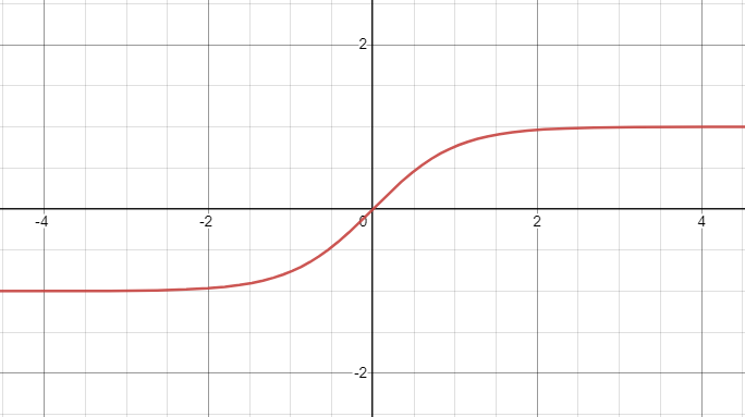
always_comb outLimit = vddMax * $tanh(outNew / vddMax);
Output stage:
Ultimately, the output stage should settle around a common voltage and exhibit high impedance if the supply or enable functions are not active.
assign outp = (shOn == 1) ? (vcm + outLimit / 2.0) : `wrealZState; assign outm = (shOn == 1) ? (vcm - outLimit / 2.0) : `wrealZState;
Results:
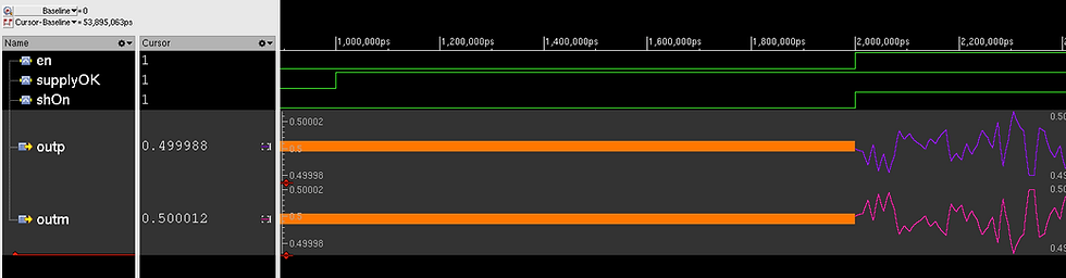
Output is High Z before supply and enable. When enable output create noise when input pins are equal.
output when the input is a sin wave, we can see the effect of limiting when output voltage reaches limiting voltage

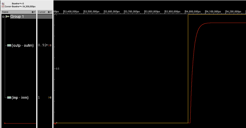
Step response due to finite bandwidth
In summary, we explored several techniques for modeling non-idealities in analog behavior. This circuit has additional non-idealities that could be considered, such as the impact of charge injection on input capacitors (even in a fully differential architecture, mismatch effects may still arise). Additionally, there are situations where you might want to model common-mode rejection ratio or the finite gain of an operational amplifier, especially in high-resolution ADCs. In my upcoming post, I will address the second stage of the pipeline ADC, which is the MDAC.
Here are a few comments.
1) You probably want a flag to turn off the noise, since calls to $dist_normal incur a non-zero processing penalty.
2) You should mention that you aren't pre-warping the pole location since the sampling rate is high enough not to matter.
3) You absolutely should filter out X and Z from your inputs, since they will kill your filter pipeline since there is no way to remove them.
Great work here.