In this blog post, I will explain the process of current sensing in flash memory cells through the utilization of Delta Sigma Modulation (DSM). The theoretical foundation for this explanation is drawn from Chapter 17 of Baker's CMOS book titled "Sensing using SD Modulation."
The organization of this post unfolds in the following manner:
1. Introduction to the fundamental concept
2. Mathematical background
3. Model of the flash cell
4. Model of the Delta Sigma Modulator (DSM)
5. Construction of the test bench
6. Presentation and analysis of results
Introduction to the fundamental concept:
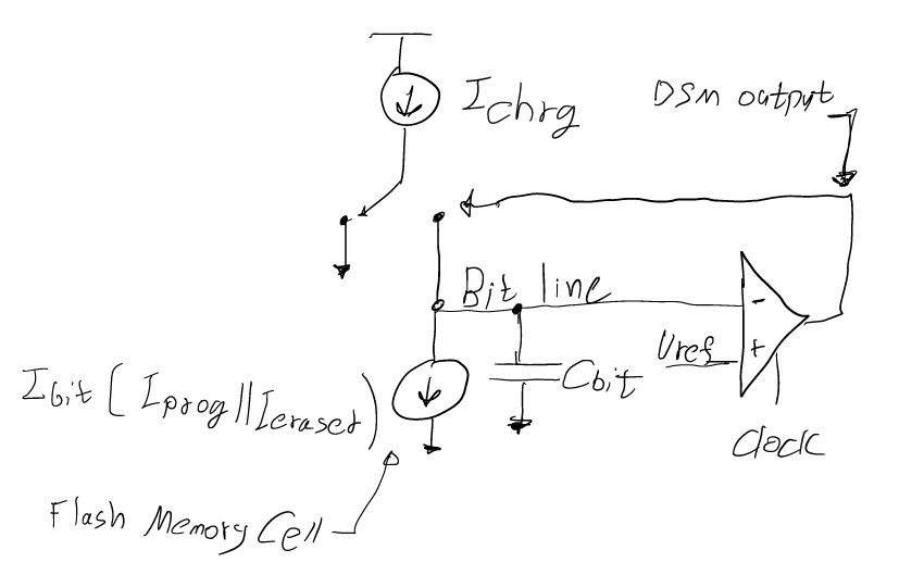
Figure 1: Sensing Flash memory cell using DSM.
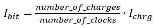
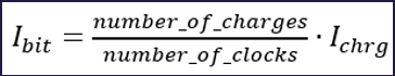
We measure the signal as the rate at which current flows out of capacitance Cbit, denoted as either Ierased or Iprog. A comparator is employed to assess whether the voltage on the bit line is below an arbitrary reference voltage, Vref. The Flash cell continually depletes charge from the bit line. When the bit line voltage falls below Vref, the current source Ichrg connects to Cbit, supplying the necessary current / charge. This connection of Ichrg elevates the voltage of Cbit. By counting the instances where Ichrg fills Cbit over the total number of clock cycles, we can estimate the value of Ibit. Consequently, we can deduce whether the Flash memory cell is in an erased or programmed state.
Figure 2 illustrates the primary signals associated with DSM Flash sensing.
Clock (green) represents the frequency at which the comparator makes decisions.
Qchrg (purple) signifies the charge exiting Cchrg as it fills Cbit.
The bit_line (red) represents the voltage across the Cbit capacitor.
Vref (blue) denotes the reference voltage.
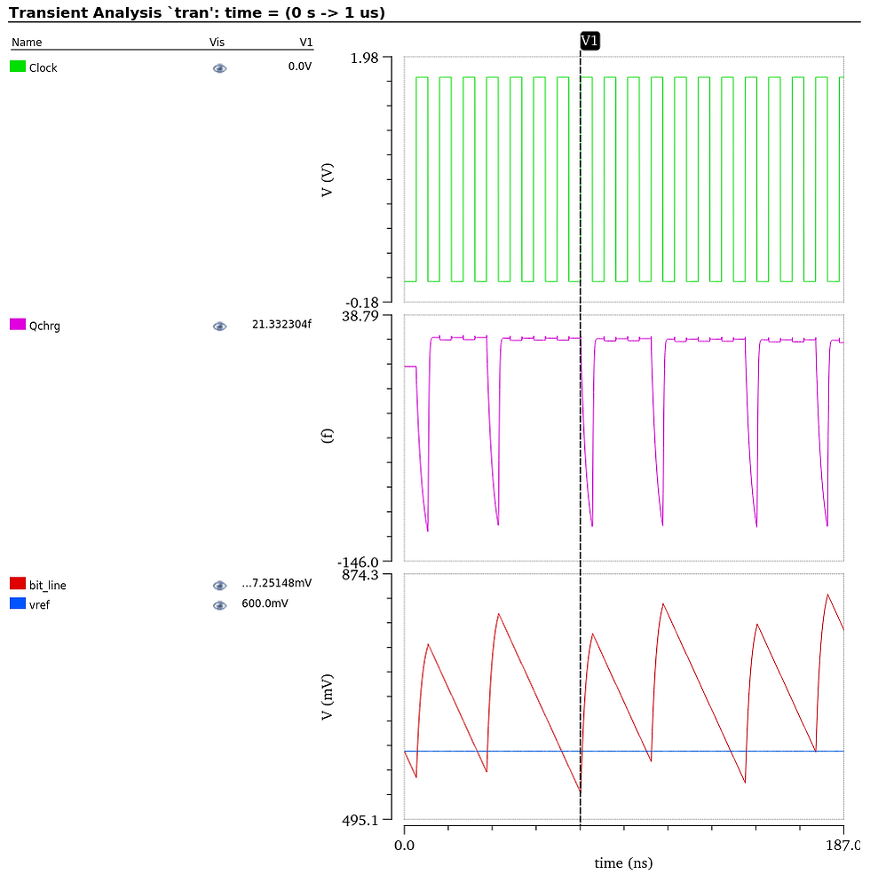
Figure 2: Primary signals associated with DSM Flash sensing.
Mathematical background:
The rate (dV/dt) at which charge is extracted from the capacitance Cbit of the bit line.

The amount of charge extracted from the bit line every clock cycle is
The charge added to Cbit by Cchrg corresponds to the instances when the comparator determined that the bit line voltage was lower than Vref, out of the total number of clock cycles that activated it.
If we set Qchrg equal to Qbit, we can derive the value of Ibit.
Model of the flash cell:
Figure 3 illustrates a sample of the current-voltage (IV) characteristics of a 3D NAND flash memory cell. It is evident that when the flash cell is in an erased state, the current flow at 0V at the gate is significantly higher compared to a programmed flash cell. We can observe a limitation on the current above a specific voltage threshold.
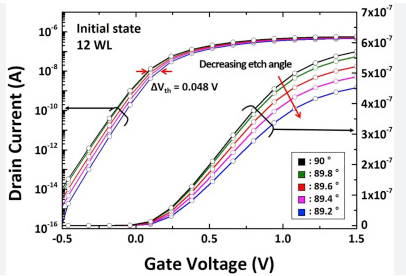
Figure 3: IV characteristics of Flash memory cell.
For this post, I represented the current conducted by the flash cell using the convenient hyperbolic tangent ($tanh) function, which restricts the cell current above a certain gate voltage.
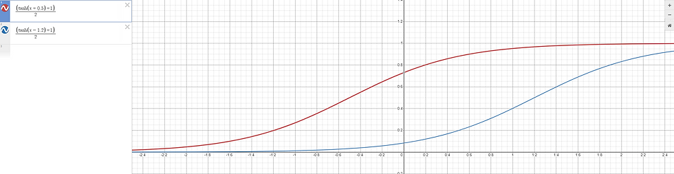
Figure 4: IV characteristics of Flash memory cell as implemented in the model.
module flashCell (vss, bit_line, row_line); inout EEnet bit_line; inout EEnet vss; input wreal1driver row_line; parameter bit state = 0; parameter real scale_curr = 10e-6;
real ibit; // The current source (sink) that remove charge from Cbit Isrc flash_dischrg(.P(bit_line),.N(vss),.ival(ibit)); // Computes the discharge current as a function of gate voltage // current is limited to scale current always begin if (state==0) begin // Erased ibit = scale_curr * ($tanh(row_line + 0.5) + 1) * 0.5; end else begin // Programmed ibit = scale_curr * ($tanh(row_line - 1.2) + 1) * 0.5; end @(row_line); end endmodule
Model of the Delta Sigma Modulator (DSM)
Pin list:
Pin name | Direction | Pin type | Function |
vdd | inout | EEnet | Supply |
vss | inout | EEnet | Ground |
bit_line | inout | EEnet | CharCbit node |
chrg_trim | input | logic[7:0] | trim the Ichrg value |
comp_ref | input | wreal1driver | comparator reference |
clk | input | logic | clock |
en | input | logic | enable |
out | output | logic[8:0] | counts the number of Ichrg instances |
module dsm (vdd, vss, bit_line, chrg_trim, comp_vref, clk, en, out); inout EEnet vdd, vss; input EEnet bit_line; input logic [7:0] chrg_trim; input logic clk; input logic en; input wreal1driver comp_vref; output logic [8:0] out;
The core structure of the DSM model involves a current source responsible for charging Cbit. The specific value of the current charging Cbit, determined by Ichrg, has been computed in subsequent sections of the code.
CapGeq #(.c(Cbit)) cBit(.P(bit_line)); Isrc_ideal iCup(.P(bit_line),.N(vss),.ival(ichrg));
In a real analog circuit, it is more effective to introduce charge to Cbit by initially charging the Cchrg capacitor and subsequently transferring this charge to Cbit if necessary. The capacitor is charged by VDD during the charge phase, and if the charge needs to be transferred to Cbit, a lower voltage is applied in the form of Vref - Vthp, where Vthp represents the threshold voltage of a PMOS transistor. Further details can be found in Chapter 17 of the book on CMOS. In our scenario, it is crucial to recognize that the current charging Cbit is influenced by the Cchrg value, Vref, Vthp, and ts, representing the allocated time for charging Cbit (typically half a clock cycle).
always begin icap = Cchrg * (vdd.V - vref - vthp) / (ts); @(vdd.V,vref); end
I incorporated a trim capability to the Vref parameter to enhance the precision of the sensed current in the flash cell.
parameter real vrefLsb = 2.0e-3; // LSB vref controlling Cchrg charge
always begin if ((supplyOK === 1'b1) && (^chrg_trim !== 1'bx) && (^chrg_trim !== 1'bz)) vref = vrefLsb * chrg_trim; @ ((supplyOK===1'b1) or chrg_trim); end
The comparator model is simple: at each clock cycle, we assess the bit line voltage. If it is below Vref, we charge Cbit with Ichrg. We keep track of the instances where the comparator decides to charge Cbit. At the conclusion of the DSM operation, we compute Ibit using the given equation. It's important to note that we reset Ichrg at the negative edge of the clock, mirroring the behavior of the actual circuit.
always @ (posedge clk) if ((enInt === 1'b1) && (supplyOK === 1'b1)) begin if (bit_line.V > comp_vref) begin ichrg = 0.0; end else begin ichrg = -1.0 * icap; count++; end end else begin ichrg = 0.0; count = 0; end // Charge is injected for half cycle only always @ (negedge clk) ichrg = 0.0;
Construction of the test bench
In the test bench, we create instances of one DSM module and one flash cell module and interconnect them. It's worth noting that in the DSM model, we have the flexibility to assign different values to the Cchrg capacitor and observe their impact on the DSM's behavior.
dsm #(.Cchrg(Cchrg)) dsm ( .vdd(vdd), .vss(vss), .bit_line(bit_line), .chrg_trim(chrg_trim), .comp_vref(comp_vref), .clk(clk), .en(en), .out(out) ); flashCell #(.state(state)) flashCell ( .bit_line(bit_line), .vss(vss), .row_line(row_line) );
We also define 2 parameters for flash cell state
`define erased 0 `define programmed 1
parameter bit state = `erased;
At the conclusion of the simulation, we determine the sensed current in the flash cell by dividing the counter output by the total number of clock cycles. It's important to highlight that we include a factor of 1/2. This adjustment is made because the transfer of charge from Cchrg to Cbit occurs only during half of the cycle, as explained in preceding paragraphs.
repeat (512) @ (posedge clk); ibit = real'(out/(2*512.0)); ibit *= expected_Chrg_charge();
function real expected_Chrg_charge(); return Cchrg * (vdd.V - vrefLsb*chrg_trim - vthp) / (ts); endfunction
Presentation and analysis of results
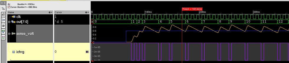
Here is the graph for an erased flash cell with Cchrg set to 200fF. The plot illustrates the sawtooth pattern of the bit_line node and illustrates how charge is introduced to the Cbit capacitor when the bit_line voltage drops below Vref.
*******************************************
For row_line voltage: 0.000V
sensed bit_line current: 7.388uA
expected bit_lined current: 7.311uA
Cchrg cap charge current: 40.240uA
*******************************************
Here is the graph for a programmed flash cell with Cchrg set to 200fF.
*******************************************
For row_line voltage: 0.000V
sensed bit_line current: 0.904uA
expected bit_lined current: 0.832uA
Cchrg cap charge current: 40.240uA
*******************************************

Here is the graph for a programmed flash cell with Cchrg set to 100fF. Notice how it takes longer to reach Vref because reduced Chrg current per cycle.
*******************************************
For row_line voltage: 0.000V
sensed bit_line current: 0.904uA
expected bit_lined current: 0.832uA
Cchrg cap charge current: 20.120uA
*******************************************
How to run this code
This code utilizes modules from the Cadence course titled "SystemVerilog Real Number Modeling (SV-RNM) Advanced Verification." I cannot include these modules in the GitHub repository due to proprietary constraints. If you wish to simulate and explore this model, please register for the course, download the database, and navigate to /SVRNM_dx/common/EEnet. Copy the files CapGeq.sv, Isrc_ideal.sv, and Isrc.sv to your cloned repository. From the tb directory, execute the command "source runEE -run -gui" to run the simulation. The GitHub repository path is provided below.
Comentários